Our Focus
Vacuum electronic devices are devices that use electrons to run in vacuum or thin gas to achieve functions. The structure includes a closed vacuum cavity, cathode and other functional components. They have a wide range of applications in military, aerospace, satellite communication, medical and health, security, lighting and other fields.
One of the key challenges for these devices is to make them smaller, more efficient and more integrated. Our laboratory has been exploring how to use micro-nano fabrication technology to achieve this goal. For instance, on-chip and integrated X-ray sources can be used for portable fluorescence instruments and other equipment. These X-ray sources can also form arrays that can improve the image quality of industrial CT and medical CT. By using micro-nano fabrication technology, we can reduce the size, power consumption and cost of vacuum electronic devices, and open up new possibilities for their applications. Our laboratory has been committed to applying micro-nano fabrication technology to vacuum electronic devices for a long time, realizing on-chip micro vacuum electronic devices.
We divide the miniaturization of vacuum electronics into three development stages: on-chip vacuum technology, on-chip vacuum electronic devices and miniature vacuum systems & devices.

1 Underlying Technologies
1.1 On-chip Electron Source
On-chip vacuum technology consists of two aspects: on-chip electron source and on-chip vacuum acquisition. The electron source is the heart of the vacuum electronic device, providing electrons for the device continuously. Traditional electron sources such as thermal emission filament and dispenser cathode are mechanically processed, which are large in size, high in power consumption and difficult to integrate, and thus not suitable for direct use in on-chip micro vacuum electronics. Our lab has developed two on-chip electron sources, on-chip thermal emission electron source and on-chip silicon oxide horizontal tunneling electron source, both of which can be prepared in bulk using micro and nano processing technology and can operate stably under low vacuum conditions, which are the preferred solutions for electron sources in on-chip vacuum electronic devices.
We have discovered that carbon nanotubes and graphene have new thermal emission mechanisms that are different from conventional hot electron emission, and we have realized the miniaturization, on-chip and arraying of hot cathodes based on semiconductor microfabrication technology, using graphene and carbon nanotubes as electron-emitting materials. Compared with the conventional hot cathode, the on-chip miniature hot electron source based on carbon nanomaterials has extremely small thermal inertia and very fast response time (<1us). With micro and nano processing techniques, on-chip miniature hot electron sources can be prepared in large scale arrays and processed at wafer level.

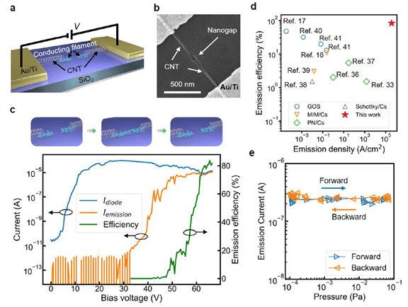
We have proposed a novel on-chip miniature electron source, a metal-insulator-metal horizontal tunneling junction electron source, and realized a $\mathrm{Si-SiO_x-Si}$ structured horizontal tunneling junction electron source on a substrate by micro and nano processing technology. The performance of the $\mathrm{Si-SiO_x-Si}$ horizontal tunneling junction electron source in terms of emission efficiency, emission current density, anti-poisoning characteristics and its microstructure are systematically investigated, and a scheme of series cascade integration and parallel large array integration is proposed to further improve its performance in terms of emission efficiency and emission current. Compared with previous on-chip electron sources (including field emission electron sources, vertical structured tunneling junction electron sources, and on-chip thermal emission electron sources), $\mathrm{Si-SiO_x-Si}$ horizontal tunneling junction electron sources can have emission efficiency and density close to those of field emission electron sources, and have comparable operating voltage and anti-poisoning characteristics to those of vertical structured tunneling junction electron sources and on-chip thermal emission electron sources, and also have simple microprocessing processes. The integrated performance of the source has significant advantages. Therefore, the horizontal tunneling junction electron source combines the advantages of conventional field emission on-chip electron source, tunneling junction electron source and on-chip thermal emission electron source, and is an on-chip electron source with balanced performance in all aspects, promising important applications in various miniature vacuum electronic devices.
1.2 On-chip Vacuum Acquisition
A complete on-chip vacuum electronic device is an individually packaged device, thus the technology of obtaining on-chip vacuum is very critical. Since a vacuum electronic device has several electrical or optical interfaces including cathode and anode, the vacuum package needs not only to achieve good gas tightness but also good sealing of the electrodes. Due to the requirement of miniaturization and the characteristics of planar process, the common way of micro-vacuum packaging is wafer bonding technology in micro-electro-mechanical system technology (MEMS), including anode bonding, silicon-silicon bonding and gold-gold bonding. Our lab has conducted continuous research in both on-chip vacuum packaging and maintenance, and has effectively improved and explored the existing bonding and electrical feedthrough technologies to successfully realize on-chip micro vacuum chambers.
2 On-chip Electronic Devices
Generally speaking, on-chip vacuum electronics refers to the realization of an individually packaged vacuum electronics device using micro and nano processing technology and MEMS process, including the cathode (electron source), vacuum environment, anode, housing and other parts.
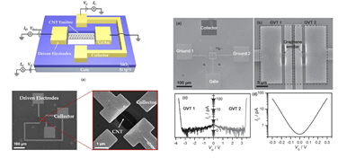
We first realized a new structure of vacuum triode using a miniature thermal emission electron source in a vacuum chamber. The vacuum transistors based on miniature thermal emission electron sources of suspended graphene or carbon nanotubes have low operating voltage (2-4 V), short response time (<1μs), high switching ratio, and good controllability. We also demonstrate the on-chip integration of graphene vacuum transistors by integrating two unipolar graphene Vacuum transistors together to realize a bipolar vacuum electronic device.
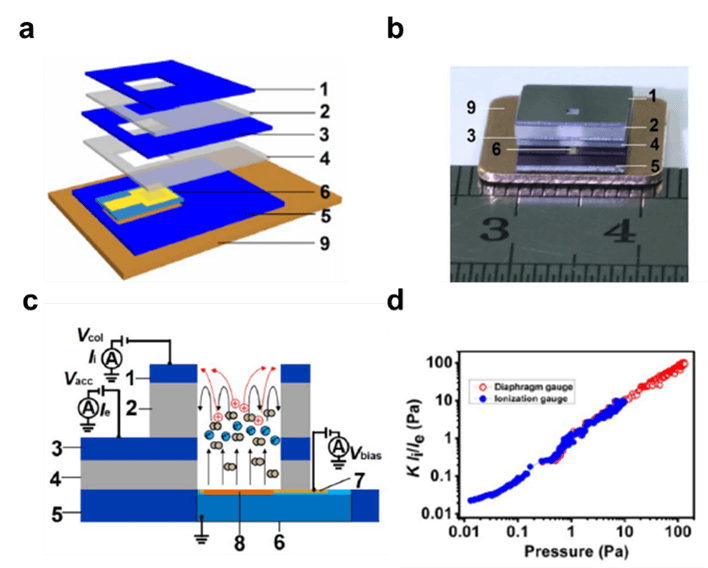
We have also fabricated an on-chip miniature ionization vacuum gauge using the MEMS technology. The ionization gauge has a size of $13 \times 9 \times 2.7 \mathrm{mm^3}$ and can probe small vacuum chambers without causing high temperature problems. The ionization gauge has a range of $1 \times 10^{-2} \mathrm{Pa}$ to $1 \times 10^2 \mathrm{Pa}$, which can be used in scenarios such as narrow vacuum devices and near-Earth satellites.
3 On-chip Vacuum System
On-chip vacuum system means miniaturization of some important vacuum devices, such as electron microscope, mass spectrometer, etc. These vacuum devices are crucial in scientific research, industry and other fields, but are large, complex systems and expensive. Most of these devices are in open structure and need inlet and outlet samples, so they cannot be separated from vacuum pumping units composed of mechanical pumps, molecular pumps or ion pumps. We hope that by using micro and nano processing technology, we can make these devices into individually packaged vacuum systems as well, removing the bloated vacuum pump sets and streamlining the system design to achieve the same function.
We believe that various technologies for miniaturization, on-chip and integration of vacuum electronic devices will gradually mature in the near future, and more and more miniature vacuum electronic devices will move from concept to reality and from laboratory to market. Our lab will seize the opportunity together with our partners to promote the development of the field of micro and nano vacuum electronic devices, to research more academic results and to create more social and economic benefits at the same time.